


I evaluated the seven best PCB design software options that stood out across G2 Grid data, user feedback, product research, and workflow fit: Altium Develop, Altium CircuitMaker, Sigrity X Platform, Allegro X PCB Designer, Autodesk Fusion, PADS Professional, and Onshape.
As I analyzed G2 reviews for this category, one thing became clear: PCB teams aren’t just comparing schematic capture or routing tools anymore. They’re trying to understand which design tools support team collaboration and design review workflows while helping them move complex boards from idea to production without avoidable rework.
That matters because PCB design decisions now stretch across more than layout. Hardware engineers need accurate simulation, signal-integrity analysis, component management, manufacturing validation, and a clean handoff between electrical, mechanical, and production teams. A tool that feels right for a solo designer may not support the depth of review, version control, or board complexity required by a larger electronics team.
The more G2 feedback I reviewed, the more I saw that each platform solves a different part of the PCB workflow. Some are strongest for collaborative electronics development, while others focus on SI/PI validation, mechanical integration, open-source projects, or manufacturing-ready output.
In this guide, I break down where each PCB design tool fits best, which strengths appeared most often in user feedback, and what buyers should consider before choosing a platform for 2026.
7 PCB design software tools that stood out during my evaluation
-
Altium Develop: Best for unified electronics development across distributed engineering teams
Combines PCB design, component management, requirements tracking, design collaboration, release workflows, and manufacturing readiness tools for organizations coordinating complex hardware projects. ($1,990/year)
-
Altium CircuitMaker: Best for community-driven PCB development and open hardware projects
Includes schematic capture, PCB layout, shared component libraries, cloud-based project collaboration, 3D board visualization, and manufacturing output tools for makers and collaborative hardware communities. (free)
-
Sigrity X Platform: Best for signal integrity and power integrity validation before manufacturing
Provides SI/PI analysis, electromagnetic simulation, design verification, impedance analysis, power distribution network modeling, and pre-production validation for high-speed electronic systems. (custom pricing)
-
Allegro X PCB Designer: Best for routing dense multilayer boards with advanced design constraints
Combines advanced PCB layout, constraint-driven routing, schematic design, high-density interconnect support, design-rule management, and large-scale board development capabilities. (custom pricing)
-
Autodesk Fusion: Best for connecting PCB design with mechanical product development
Brings together electronics design, 3D modeling, enclosure development, simulation, manufacturing workflows, and ECAD-MCAD collaboration within a unified engineering environment. ($57/month)
-
PADS Professional: Best for accelerating complex PCB layout and routing workflows
Offers schematic capture, advanced routing, constraint management, design validation, multi-board development support, and engineering productivity tools for sophisticated PCB projects. (custom)
-
Onshape: Best for browser-based engineering collaboration and design version control
Includes cloud-native CAD, real-time collaboration, version management, design review workflows, product development coordination, and secure engineering data management. ($1,500/user/year)
*These PCB design software tools are top-rated in their category, according to the latest G2 2026 Summer Grid Report shared for this article. I’ve added their standout features and pricing information for easy comparison.
7 best PCB design software tools I recommend for electronics and hardware engineering teams
As I analyzed G2 reviews in this category, I noticed that PCB design teams rarely evaluate software solely on routing capabilities. The most common buying considerations extended into collaboration, simulation accuracy, component management, manufacturing readiness, and how easily designs could move between electrical and mechanical engineering workflows.
That broader demand is reflected in the market itself. The global PCB design software market is projected to grow from $4.12 billion in 2025 to $13.32 billion by 2034, creating a more crowded landscape for buyers comparing the best PCB design software for their specific requirements.
As I reviewed G2 feedback, another pattern emerged: the strongest products weren’t trying to solve every engineering challenge. Some stood out for signal integrity validation, while others excelled at collaborative electronics development, cloud-based design management, or connecting PCB workflows with mechanical design processes. Teams exploring adjacent design workflows may also benefit from evaluating other free CAD software for engineers.
The tools below earned their place because each addresses a distinct PCB design challenge, making them stronger fits for different engineering teams, board complexities, and product development workflows.
How I found and evaluated the best PCB design software
I started with G2’s latest Grid Reports to identify platforms with strong satisfaction scores, market presence, and consistent review activity. Because PCB design software serves a wide range of engineering needs — from schematic capture and board layout to signal integrity analysis, manufacturing validation, and design collaboration — I focused on products that solved a distinct challenge particularly well.
As I worked through the shortlist, I found that the best PCB design software wasn’t defined by feature volume alone. Some platforms excelled at managing complex multilayer boards, while others stood out for simulation accuracy, electronics development workflows, or cloud-based collaboration. Understanding those differences helped shape my evaluation process.
To better understand real-world performance, I used AI to analyze verified G2 reviews at scale. This allowed me to identify recurring strengths, workflow patterns, and common considerations that surfaced across different engineering teams. I paid close attention to feedback around routing capabilities, design-rule management, simulation quality, manufacturing readiness, and most reliable PCB design software by electrical engineers based on user reviews.
The final list reflects a combination of G2 review analysis, category data, product research, and workflow fit. Screenshots featured throughout this article come from G2 vendor profiles and publicly available product documentation.
What makes the best PCB design software: My criteria
As I analyzed G2 reviews and Grid data, I found that category requirements were only the baseline. The strongest platforms helped engineering teams move from PCB layout and schematic design to manufacturing-ready boards with stronger accuracy, collaboration, and design confidence.
These seven products performed strongest across the following evaluation areas:
- PCB layout and routing flexibility: Since PCB design complexity varies widely between projects, I prioritized tools that could support everything from straightforward board layouts to dense multi-layer designs. The strongest products combined automated routing capabilities with enough control to fine-tune critical signal paths and board constraints.
- Schematic design and electrical accuracy: Because schematic editing is a core category requirement, I looked closely at how effectively each platform handled component connectivity, net management, electrical rule validation, and design consistency throughout the development process.
- Component library quality and footprint management: I gave more weight to products that made component selection and footprint implementation easier. Strong libraries, customizable footprints, supplier data integration, and efficient component management all contributed to a smoother design workflow.
- Signal integrity and design validation: Modern PCB projects often involve increasingly complex electrical requirements. I favored tools that helped teams validate designs through simulation, signal integrity analysis, power integrity checks, and pre-manufacturing verification before committing to production.
- Mechanical design and engineering interoperability: PCB development rarely happens in isolation. I evaluated how well products connected with broader CAD software and MCAD software workflows, helping teams coordinate electrical and mechanical design decisions more effectively.
- Collaboration and design review workflows: Engineering projects typically involve multiple stakeholders across design, validation, and manufacturing. Products stood out when they supported version control, design reviews, change tracking, and collaboration without creating unnecessary workflow friction.
- Long-term usability and workflow fit: The best PCB design software should continue delivering value long after the first design is completed. I looked for products that G2 reviewers consistently associated with efficient day-to-day workflows, dependable performance, manageable implementation effort, and strong adoption across engineering teams.
The list below contains genuine user reviews from the PCB design software category page. To qualify for inclusion in the category, a product must:
- Modify PCB layouts and PCB circuitry
- Include a components library so users can easily implement high-quality PCB footprints
- Provide schematic editing tools for modification of electrical properties and other attributes of components, wires, nets, and pins.
*This data was pulled from G2 in 2026. Some reviews may have been edited for clarity.
1. Altium Develop: Best for unified electronics development across distributed engineering teams
One theme kept resurfacing as I analyzed G2 reviews for Altium Develop: teams weren’t adopting it simply to create PCBs. They were using it to keep engineering work connected. Reviewers frequently described situations where schematic design, board layout, component management, design reviews, and manufacturing preparation all needed to move together without becoming separate workflows. That broader engineering continuity is what gives Altium Develop a distinct position in the category.
The category data reflects that confidence. Altium Develop holds a 4.5-star rating across 900+ reviews, with 97% of users rating it four or five stars and 90% saying they would recommend the platform. As I compared those numbers against the broader PCB Design category, I found that reviewers often associated the platform’s value with consistency across projects rather than isolated design features.
PCB design itself remains one of its strongest foundations. PCB layout editing, layers, and schematic editor all earned scores above 90%, and reviewers regularly highlighted routing flexibility, trace management, design organization, and layout efficiency. The feedback suggests that Altium Develop performs particularly well when projects grow beyond straightforward board designs and require tighter control over increasingly complex electrical systems.
Component management emerged as another recurring advantage. Several reviewers discussed reusable libraries, supplier information, BOM workflows, and centralized design assets as practical ways to reduce repetitive work. As I reviewed the feedback, it became clear that these capabilities help teams maintain consistency across multiple projects while reducing the effort required to manage large component ecosystems.
Mechanical collaboration appeared just as frequently. Reviewers referenced STEP imports, enclosure validation, and smoother coordination with engineering teams working in general-purpose CAD software. Rather than treating PCB design as an isolated activity, many users described tasks where electrical and mechanical decisions could be reviewed together earlier in the development cycle.
The platform’s visualization capabilities also received consistent praise. Multiple reviewers highlighted 3D board views and design-review workflows that helped teams validate fit, orientation, and assembly considerations before manufacturing. For organizations that regularly work alongside broader 3D modeling software environments, that visibility can help reduce costly revisions later in the product development process.
As I worked through the reviews, I also noticed how frequently users connected Altium Develop to larger engineering initiatives. Simulation, design validation, procurement planning, and manufacturing preparation were often discussed alongside core PCB functionality. That combination helps explain why many teams evaluating the highest rated PCB design for complex boards, ensuring first software-time manufacturing success rates, continue to shortlist Altium Develop for sophisticated hardware programs.
Anyone who wants to benefit from structured engineering workflows, Altium Develop is a good choice. Teams working on smaller projects may spend additional time evaluating subscription options, workspace controls, and collaboration settings before fully benefiting from the platform. For larger engineering groups, those same controls often support stronger project governance and review processes.
The platform also performs best when teams are prepared for a more comprehensive environment. Some reviewers mentioned performance slowdowns, autosave concerns, and onboarding considerations tied to advanced functionality. For organizations managing complex development efforts, those factors appeared to be implementation considerations rather than reasons to abandon the platform.
Altium Develop is a strong fit for engineering organizations that need PCB design, component management, mechanical coordination, and project collaboration to function as part of a connected workflow. Its greatest value comes from helping teams maintain continuity across the product development process while supporting increasingly sophisticated board designs.
What I like about Altium Develop:
- One capability that stood out across the G2 reviews I analyzed was Altium Develop’s ability to keep PCB design, component management, and engineering collaboration connected throughout the development process.
- The G2 feedback I reviewed frequently highlighted the combination of advanced PCB design tools, design review workflows, and mechanical integration capabilities for complex hardware projects.
What G2 users like about Altium Develop:
“What I consider the most helpful thing about Altium Develop is the built-in version control and structured collaboration it brings to hardware design. It makes it much easier to track changes, manage revisions, and see who modified what without relying on manual file naming or shared drives. I don’t have to worry about losing changes, overwriting someone else’s work, or digging through old file versions to figure out what happened. Everything is tracked clearly, and collaboration feels more organized. Since it works directly within Altium Designer through Altium 365, it feels like a seamless part of the design process rather than an extra tool to maintain. Overall, it just makes teamwork smoother and reduces the friction that usually comes with managing complex PCB projects.”
– Altium Develop review, Efren Z.
What I dislike about Altium Develop:
- For smaller teams, the review patterns I analyzed suggest that evaluating subscription tiers, workspace permissions, and collaboration controls can require additional planning.
- As projects become more advanced, G2 reviewers occasionally reference onboarding and performance considerations that may benefit from clearly defined processes before broader adoption.
What G2 users dislike about Altium Develop:
“The only issues I have ran into so far are crashes and the autosave function failing. At times, it will freeze up randomly even if there was no input into the program. Additionally, the autosave feature is not the greatest, as it doesn’t always reconnect to the host server. I actually lost a small amount of work from yesterday due to this.”
– Altium Develop review, Charlie K.
Engineering teams often rely on multiple design systems throughout product development. Understanding how CAD data exchange works can help reduce friction when design information moves between electrical, mechanical, and manufacturing environments.
2. Altium CircuitMaker: Best for community-driven PCB development and open hardware projects
Professional PCB software asks users to pay before they know how deep their projects will become. Altium CircuitMaker stood out to me in the G2 feedback because it lowers that barrier. Reviewers described it as a practical way to learn PCB design habits, build open hardware projects, and access Altium-style workflows without an enterprise software budget.
The product data supports that access-first story. CircuitMaker holds a 4.3-star rating across 100+ reviews, with 94% of users rating it four or five stars and 86% saying they would recommend it. Ease of setup scored 90%, while schematic editor reached 90%, PCB layout editing scored 89%, and component placement came in at 88%. Those numbers match the reviewer pattern I kept seeing: approachable, capable, and useful.
Learning value carried through many reviews I read. Users described the interface as intuitive, especially for students, interns, hobbyists, and engineers building PCB experience. Because the platform shares design concepts with Altium’s broader ecosystem, it helps users practice schematic capture, layout editing, component placement, and design organization before moving into advanced tools.
Community support gives CircuitMaker a personality of its own. G2 reviewers pointed to forums, shared projects, and community knowledge as meaningful parts of the experience. That makes the platform feel aligned with open hardware projects, where learning, reuse, and shared troubleshooting matter as much as the board file.
G2 reviewers also called out visualization and validation features. The 3D viewer, design-rule checking, and board visualization help users inspect layouts before fabrication. CircuitMaker is not a substitute for specialized simulation and CAE software, but the feedback suggests its built-in checks give makers a clearer path to manufacturable boards.
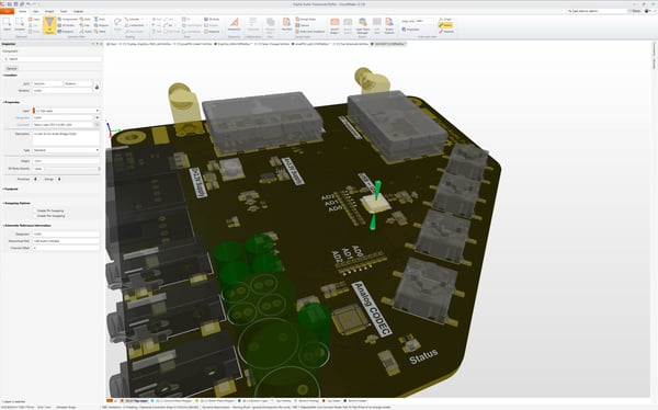
The free pricing model remained a reason users valued the product. Reviewers connected that accessibility to experimentation, training, and independent engineering work. For buyers comparing the best PCB design software with budget constraints in mind, CircuitMaker’s schematic capture, PCB layout tools, and community resources give it a distinct role.
Manufacturing handoffs appeared more often than I expected for a free, community-focused platform. Users discussed board validation, output preparation, and PCB design platforms with seamless CAM output for manufacturing handoff for your workflow in practical terms. CircuitMaker may not target enterprise release management, but reviewers described it as capable enough for fabrication-oriented work.
CircuitMaker’s cloud-centered model shapes where it fits best. Users who like automatic syncing, shared access, and public project collaboration often benefit from that structure. Privacy-sensitive teams, offline workflows, or users who want local ownership may need to evaluate whether the cloud model aligns with their project requirements.
Platform flexibility is another fit consideration. The tool is built around Windows workflows, so macOS or Linux users may need a virtual machine to access it. For its core audience, that setup can be acceptable when free access and community learning matter most.
CircuitMaker works best when accessibility is the deciding factor. It is not trying to replace enterprise PCB systems for advanced teams. Its value comes from giving students, makers, open-hardware contributors, and cost-conscious engineers a path into PCB design without losing the community support that helps them improve.
What I like about Altium CircuitMaker:
- The G2 reviews I analyzed frequently highlighted Altium CircuitMaker’s ability to make professional PCB design workflows more accessible without sacrificing core functionality.
- Many users on G2 praised the combination of community resources, board visualization tools, and design-rule checking for supporting learning and open hardware development.
What G2 users like about Altium CircuitMaker:
“The user interface is intuitive, and anyone can start hands-on with a minimal learning curve. The tools are great for even some industrial projects. It’s a perfect step to start the journey to Professional PCB design, as it is built on the foundation of Altium Designer. It inherits the robust features of Schematic capture, PCB Layout, and 3D visualization. One of the greatest strengths is its active and supportive community forum, which has helped me enhance my learning and troubleshooting experience. For its no-cost entry point, we have quite frequently opted for CircuitMaker to train interns and students just getting started, and the projects that are created can be easily migrated and integrated with Altium Professional.”
– Altium CircuitMaker review, Om B.
What I dislike about Altium CircuitMaker:
- Offline project ownership comes up periodically in G2 reviews. Teams that prefer keeping design files locally may find CircuitMaker’s cloud-first approach less aligned with their workflow preferences.
- G2 reviewers frequently position CircuitMaker as a learning and community-focused platform. As engineering requirements become more specialized, some users eventually describe needing deeper workflow controls and project management capabilities.
What G2 users dislike about Altium CircuitMaker:
“Creating new/custom components can feel a little buggy, and if you import a component that was made with a different grid spacing, circuit design can end up a little cumbersome. The only other area of friction is having everything saved through the cloud which can be an issue if I’m working away from my desk and internet connection.”
– Altium CircuitMaker review, Christian G.
3. Sigrity X Platform: Best for signal integrity and power integrity validation before manufacturing
Many PCB tools focus on board design. Sigrity X Platform focuses on proving that the board will behave as expected before it is built. As I worked through the G2 reviews, I found that users consistently described the platform as an engineering validation environment rather than a traditional PCB design application. The conversations were rarely about placing components or routing traces. Instead, they centered on signal integrity, power integrity, simulation accuracy, and reducing expensive surprises later in the development cycle.
The category data reflects that specialized positioning. Sigrity X Platform has a 4.2-star rating across 30+ reviews, with 90% of users rating it 4 or 5 stars and 84% saying they would recommend it. While its overall satisfaction score trails some PCB design products, it also holds the largest market presence in the category and appears in the simulation & CAE category, reinforcing its role as a validation-focused platform.
One theme appeared almost immediately in the reviews I analyzed: engineers trust Sigrity X to answer difficult electrical questions before hardware exists. Reviewers repeatedly highlighted signal integrity analysis, power integrity analysis, impedance verification, crosstalk evaluation, and PDN behavior modeling as capabilities that help uncover issues before prototypes are manufactured.
The platform’s simulation depth received similar praise. Several reviewers described using Sigrity X to evaluate high-speed interconnects, package designs, and complex PCB architectures that would be difficult to validate through basic rule checking alone. In many cases, users framed simulation as a way to reduce design iterations rather than simply verify designs after the fact.

Performance also surfaced as a meaningful differentiator. I found repeated references to distributed computing, parallel simulations, and significantly faster analysis times for large projects. For organizations working on dense, high-speed electronics, simulation speed appears to directly affect engineering productivity and validation cycles.
Integration within the Cadence ecosystem was another recurring advantage. Multiple reviewers discussed moving between layout, extraction, simulation, and analysis workflows without switching between disconnected tools. That continuity helps engineering teams evaluate complex electrical behavior without constantly exporting and reimporting design data.
Several G2 reviewers also connected Sigrity X to manufacturing readiness. By identifying SI and PI issues early, engineers described reducing re-spins, prototype costs, and debugging effort later in development. Those benefits are especially relevant for teams evaluating the best PCB design software for hardware engineers designing complex circuit boards, where a single design issue can introduce significant delays.
The platform’s value is particularly evident when projects involve high-speed electronics, advanced packaging, or demanding signal-performance requirements. Reviewers repeatedly emphasized that deeper analysis helps uncover issues that standard design checks may never reveal. In scenarios where error detection in data transmission and electrical reliability directly affect product performance, that additional visibility becomes a meaningful advantage.
Sigrity X is designed for engineers who regularly work with sophisticated electrical systems. Teams focused on simpler PCB projects may spend time configuring workflows and simulation models that exceed the needs of their designs. For organizations managing advanced SI and PI challenges, that depth is often the reason they adopt the platform in the first place.
The feedback also suggests that the platform rewards experience. Several reviewers mentioned onboarding effort, interface complexity, and simulation setup requirements, particularly when configuring large or multi-board environments. For teams already invested in detailed electrical analysis, those considerations seemed more closely tied to platform depth than to dissatisfaction with its capabilities.
Rather than replacing PCB design tools, Sigrity X complements them. Its greatest value lies in helping engineering teams understand how complex designs will perform before committing to fabrication, reducing uncertainty between design completion and production. That role makes it especially relevant for organizations where reliability, performance, and first-pass success carry significant business impact.
What I like about Sigrity X Platform:
- Based on the G2 reviews I analyzed, Sigrity X delivers its greatest value through deep SI and PI visibility. Reviewers consistently highlighted its ability to uncover electrical issues before fabrication, reducing re-spins and downstream troubleshooting effort.
- According to G2 reviewers, simulation speed and integration are major strengths. Teams frequently referenced faster validation cycles, distributed computing capabilities, and smoother movement between design and analysis workflows.
What G2 users like about Sigrity X Platform:
“Sigrity X Platform is most helpful when working on complex PCB designs where signal integrity, power integrity, and high-speed performance matter. What I like best is that it gives engineers a much deeper view into how the board will behave before hardware is manufactured, which helps reduce the risk of costly respins.
The UI is fairly structured once you understand the workflow, and the integration with the Cadence ecosystem is a major benefit. Being able to move between layout, extraction, simulation, and analysis in a connected environment makes the process more efficient than using several disconnected tools. Performance is also a strong point, especially when dealing with larger and more detailed designs. The simulation capability is powerful for analysing PDN behaviour, crosstalk, impedance issues, timing concerns, and high-speed interconnects.
Overall, Sigrity X is a strong platform for serious SI/PI work. It is best suited for engineers and organizations dealing with high-speed PCB designs where reliability, performance, and first-pass success are important.”
– Sigrity X Platform review, Rohan H.
What I dislike about Sigrity X Platform:
- Several G2 reviewers indicated that Sigrity X delivers the most value when teams regularly perform advanced electrical analysis. Organizations working on straightforward PCB designs may find that their simulation depth exceeds what they need day to day.
- Based on the feedback I reviewed, setup, configuration, and workflow management can require additional preparation, particularly for large-scale or multi-board projects. Teams should account for onboarding and process development when introducing the platform into existing validation workflows.
What G2 users dislike about Sigrity X Platform:
The setup process feels clunky for multi-fabric designs. Configuring connection ports and mapping models across separate package-to-board interfaces can be finicky, and it sometimes results in vague error logs. That ends up pushing us to spend extra time troubleshooting the tool instead of focusing on the data analysis. Clearer, more descriptive error messages and smarter automated pin-mapping would make the workflow smoother and save a lot of time.
– Sigrity X Platform review, Om U.
4. Allegro X PCB Designer: Best for routing dense multilayer boards with advanced design constraints
The first thing that stood out as I analyzed the G2 reviews for Allegro X PCB Designer was how often users talked about control. Many PCB platforms focus on making design easier, but Allegro X appears focused on giving engineers greater precision over increasingly complex layouts. Reviewers frequently referenced dense multilayer boards, advanced routing requirements, electrical constraints, and signal analysis workflows that would be difficult to manage in simpler PCB environments.
The category data reflects that positioning. Allegro X PCB Designer holds a 4.4-star rating across 30+ reviews, with 93% of users rating it four or five stars and 87% saying they would recommend it. It also earned strong satisfaction scores for meets requirements (93%), quality of support (92%), ease of use (91%), and ease of setup (90%), suggesting that users find the platform approachable despite its depth.
Routing capabilities emerged as one of the most consistent strengths in the feedback I reviewed. Layers, schematic editor, and PCB layout editing all earned 94% satisfaction scores, making them the highest-rated features in the category data. Reviewers regularly described creating complex schematics, managing intricate layouts, and maintaining design accuracy across demanding projects.
I also found repeated praise for design analysis and validation workflows. Multiple reviewers discussed signal integrity analysis, electrical analysis, thermal analysis, eye-diagram evaluation, and debugging capabilities. Rather than treating analysis as a separate engineering task, users often described it as an integrated part of the design process that helped identify issues earlier.
Manufacturing preparation surfaced throughout the reviews as well. Engineers referenced floor planning, auto-placement, auto-routing, Gerber generation, and design verification workflows that helped move projects toward production. For teams evaluating circuit board design platforms with accurate simulation and manufacturing validation for your team, Allegro X consistently appeared in conversations about reducing design risk before fabrication begins.
Database and library management emerged as another practical advantage. Several reviewers highlighted component libraries, BOM management, and integrated design data as useful ways to maintain consistency across projects. Those capabilities become particularly valuable when Allegro X is paired with broader PLM solutions for product development teams, where engineering data must remain synchronized across multiple stakeholders.
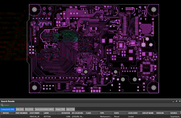
Another pattern I noticed involved error identification. Users frequently discussed constraint management, electrical rule verification, signal analysis, and debugging tools that helped uncover issues before they became production problems. That emphasis on validation reinforces why many teams include Allegro X when comparing the best PCB design software for sophisticated electronics development.
The platform is designed for engineers who want significant control over routing, constraints, and analysis workflows. Teams working on straightforward board designs may not always need the same level of configuration flexibility. For organizations managing dense multilayer boards, those capabilities often become a competitive advantage rather than additional complexity.
Reviewers also noted that extracting maximum value from Allegro X can require familiarity with its workflow structure. Setup, navigation, and advanced feature usage occasionally require additional ramp-up time, particularly for users transitioning from simpler PCB design environments. For engineering teams that regularly work on complex projects, that investment often aligns with the platform’s broader capabilities.
Allegro X PCB Designer excels when precision, scalability, and validation matter as much as routing itself. Its strongest value comes from helping engineers manage sophisticated board designs while maintaining visibility into performance, manufacturability, and design constraints throughout the development process.
What I like about Allegro X PCB Designer:
- One capability that stood out across the G2 reviews I analyzed was Allegro X’s combination of advanced routing and design validation, which reviewers frequently linked to greater confidence when managing dense multilayer PCB designs.
- G2 feedback consistently highlights the platform’s ability to bring schematic design, analysis, library management, and manufacturing preparation into a connected engineering workflow.
What G2 users like about Allegro X PCB Designer:
“Many complex and low-complexity designs can be reduced in design time using this software. We can easily track the errors or some issues. Allegro PCB designer also support advanced SI features to simulate.”
– Allegro X PCB Designer review, Prajwal V.
What I dislike about Allegro X PCB Designer:
- Experience level is a recurring theme in G2 reviews. Engineers transitioning from simpler PCB design tools may need additional time to become comfortable with Allegro X’s advanced capabilities.
- As projects become larger and more complex, G2 reviewers occasionally reference performance and workflow-efficiency considerations, particularly when working with extensive analysis or legacy design processes.
What G2 users dislike about Allegro X PCB Designer:
“Certain parts were a little confusing, and it took time to ramp up and learn what did what.”
– Allegro X PCB Designer review, Daniel C.
Understanding how computer-aided manufacturing (CAM) software supports manufacturing handoff can help explain why PCB teams place so much emphasis on clean Gerber generation, validation workflows, and production-ready design outputs.
5. Autodesk Fusion: Best for connecting PCB design with mechanical product development
Most PCB design tools stop at the board. Autodesk Fusion stood out to me because reviewers consistently described workflows that continue well beyond PCB layout. As I analyzed the G2 feedback, I found engineers using Fusion to move between electronics design, mechanical modeling, simulation, manufacturing preparation, and product development without constantly switching platforms. That broader workflow is what makes Fusion different from many products in this category.
The category data supports that versatility. Autodesk Fusion holds a 4.5-star rating across 500+ reviews, with 97% of users rating it four or five stars and 89% saying they would recommend it. It also earned strong scores for meets requirements (91%), ease of doing business with (90%), component placement (89%), and 3D modeling tools (92%). Those numbers align closely with the themes that surfaced throughout the reviews I examined.
Mechanical integration emerged as the clearest differentiator. Multiple reviewers discussed designing parts, assemblies, enclosures, and PCB-related components within the same environment. Rather than treating electronics and mechanical development as separate disciplines, Fusion gives teams a shared workspace where design decisions can be evaluated together before production begins.
The CAD-to-CAM workflow received similar praise. Users repeatedly referenced moving from design into manufacturing preparation without exporting projects between disconnected systems. As I reviewed the feedback, I found that engineers frequently described rapid design changes, machining preparation, and production planning as part of the same process. That connection becomes especially valuable for teams that rely on prototyping software to validate concepts before committing to manufacturing.
Parametric modeling also surfaced as a recurring strength. Reviewers highlighted the ability to modify dimensions, update designs, and propagate changes throughout assemblies without rebuilding models from scratch. That flexibility helps teams iterate more quickly when product requirements evolve or mechanical constraints change.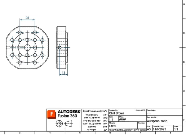
Another theme that appeared consistently was accessibility. Students, hobbyists, startups, and professional engineering teams all described finding value in Fusion. Some reviewers specifically mentioned educational licensing, free-tier access, and a relatively approachable interface compared with traditional CAD systems. That combination broadens Fusion’s appeal beyond experienced CAD specialists.
Simulation and validation capabilities were frequently mentioned as well. Engineers discussed testing designs, reviewing manufacturing readiness, and validating concepts before production. For teams evaluating which PCB design software provides signal integrity analysis and design validation for your workflow, Fusion offers broader design-validation support even though its primary focus extends beyond dedicated SI and PI analysis.
Cloud collaboration contributes to that workflow flexibility. Several reviewers appreciated version tracking, shared access, automatic updates, and the ability to work across locations. As I reviewed the feedback, I noticed that many users also valued how Fusion maintains project continuity through cloud storage and synchronization. Teams already familiar with concepts such as cached data may find it easier to understand how local and cloud-stored information interact during day-to-day design work.
Fusion is built around a connected, cloud-enabled development experience. Teams that benefit from collaboration, version management, and centralized project access often gain the most value from that approach. For users who frequently work offline or require complete local control of design files, the cloud dependency can require additional planning before adoption.
The platform also works best when hardware resources and workflow expectations align with project complexity. Some reviewers noted that large assemblies, advanced simulations, and frequent updates can occasionally affect responsiveness or require adjustment periods. For organizations using Fusion across product design and manufacturing workflows, those considerations typically appeared alongside otherwise positive experiences.
Fusion’s strongest contribution is not PCB design alone. It is the ability to connect PCB development, mechanical engineering, manufacturing preparation, and product iteration within a single environment. That broader perspective makes it particularly valuable for teams building complete products rather than individual circuit boards.
What I like about Autodesk Fusion:
- The G2 reviews I analyzed frequently highlighted Fusion’s ability to connect CAD, PCB design, simulation, and manufacturing workflows within a single platform.
- A recurring strength in G2 feedback was the combination of parametric modeling, mechanical design, collaboration tools, and manufacturing preparation that supports end-to-end product development.
What G2 users like about Autodesk Fusion:
“What I like best about Autodesk Fusion is that it brings design, simulation, and manufacturing into a single platform, which makes the entire workflow smooth and efficient. I can create a 3D model, make quick design changes, and directly test or prepare it for manufacturing without switching between multiple software tools. The parametric modeling feature is especially helpful because it allows easy edits even at later stages of the design. I also like the clean and intuitive interface, which makes it beginner-friendly while still offering advanced tools for complex designs. For students and engineers, the availability of cloud saving and collaboration makes project work more organized and accessible from anywhere. The best part for me about Fusion 360 is that you can design whole Electronic components in 3D , also we can design PCBs and use the auto routing feature all in a single platform.”
– Autodesk Fusion review, Vivek S.
What I dislike about Autodesk Fusion:
- Cloud-based collaboration is a recurring topic in G2 reviews. Teams that regularly work offline or require complete local control over project files may need to account for that dependency.
- As projects become larger and more simulation-intensive, G2 reviewers occasionally reference workflow adjustments related to hardware performance and product updates.
What G2 users dislike about Autodesk Fusion:
“Autodesk has been trimming down the free tier, which is pretty sad because fewer people will have the chance to learn with real-world tools as I did. I also think it kind of has an excessive cloud dependency. If I want to work offline, I’m stuck.”
– Autodesk Fusion review, Jasson C.
6. PADS Professional: Best for accelerating complex PCB layout and routing workflows
Speed means different things in PCB design. For some teams, it’s about finishing layouts faster. For others, it’s about reducing the number of design cycles required to reach production. As I analyzed the G2 reviews for PADS Professional, I found that users frequently connected the platform to both goals. The feedback focused less on flashy features and more on practical engineering efficiency: routing boards faster, validating decisions earlier, and maintaining control as designs become more complex.
PADS Professional holds a 4.1-star rating across 60+ reviews, with 89% of users rating it four or five stars and 82% saying they would recommend it. It also earned strong scores for ease of doing business with (92%), quality of support (89%), layers (88%), component placement (88%), and meets requirements (86%). Those metrics align closely with the experiences reviewers described throughout the feedback I examined.
Routing capabilities emerged as one of the platform’s most consistent strengths. Several reviewers highlighted sketch routing, auto-routing assistance, rigid-flex support, and advanced layout functionality designed for dense PCB projects. Rather than replacing engineer judgment, users often described these tools as ways to accelerate repetitive work while maintaining design control.
Simulation and validation appeared throughout the reviews as well. Multiple users referenced built-in simulation tools, constraint-driven design, HyperLynx integration, signal integrity analysis, and power integrity workflows. As I reviewed the feedback, it became clear that many engineers view PADS Professional as more than a layout tool. It also serves as a platform for identifying issues before they become manufacturing problems.
That theme surfaced repeatedly when reviewers discussed design accuracy. Constraint management, pre-layout validation, post-layout analysis, and routing verification were frequently connected to fewer redesigns and stronger outcomes. For teams asking what are the best PCB design tools for electronics teams reducing design iterations, PADS Professional consistently appeared in conversations about catching problems earlier in the development process.
Library and component management represent another practical advantage. Several reviewers discussed reusable components, database connectivity, part creation workflows, and variant management. Those capabilities help teams maintain consistency across projects while reducing the effort required to manage evolving design libraries.
The platform also fits naturally into broader engineering workflows. Users referenced documentation, project handoffs, and collaboration processes that extend beyond PCB layout itself. Organizations already using engineering document management software may find it easier to maintain traceability between design decisions, project documentation, and manufacturing deliverables.
Version control surfaced in a different way than it does with cloud-first PCB platforms. Rather than emphasizing collaboration features, reviewers focused on maintaining design consistency and managing project evolution over time. That makes integration with broader version control software environments particularly relevant for teams handling multiple revisions or long-lived product lines.
PADS Professional is built for engineers who need advanced PCB functionality without moving into more specialized enterprise platforms. Teams working primarily on straightforward layouts may not require the same depth of routing, simulation, and constraint-management capabilities. For organizations handling increasingly complex boards, those features often become part of the platform’s value.
The feedback also suggests that onboarding can require some patience. Several reviewers mentioned interface familiarity, workflow navigation, documentation gaps, and setup considerations when adopting the platform. For engineering teams investing in advanced PCB development workflows, those factors generally appeared as implementation considerations rather than barriers to long-term use.
PADS Professional earns its place through practical engineering efficiency. Its strongest value comes from helping teams move complex PCB designs from schematic through validation and layout while maintaining the control needed to minimize redesigns and support production-ready outcomes.
What I like about PADS Professional:
- G2 reviews frequently point to PADS Professional’s balance of advanced routing and design validation as a reason engineers can move complex PCB projects forward more efficiently.
- Simulation workflows, HyperLynx integration, and constraint-driven design also stand out in G2 feedback for helping teams catch design issues earlier.
What G2 users like about PADS Professional:
“It provides advanced routing automation, rigid-flex design capabilities, and multi-point signal integrity simulation to streamline hardware development. Also, its new AI features helped me to save a lot of time.”
– PADS Professional review, Mohit J.
What I dislike about PADS Professional:
- The learning curve appears regularly in G2 reviews, especially for engineers moving from simpler PCB tools into PADS Professional’s more advanced workflow structure.
- Documentation, interface navigation, and workflow customization also come up in G2 feedback as areas where larger engineering teams may need clearer standards and training.
What G2 users dislike about PADS Professional:
“The interface and workflow are not very intuitive for new users. It takes significant time to understand the navigation, settings, and advanced features compared to some modern PCB tools.”
– PADS Professional review, Chandra Prakash V.
7. Onshape: Best for browser-based engineering collaboration and design version control
Most engineering platforms ask teams to adapt their workflows around files. Onshape approaches the problem differently. As I worked through the G2 reviews, I found that users rarely started by talking about modeling tools or CAD features. Instead, they talked about access. They talked about opening projects from any device, sharing designs instantly, tracking revisions without manual file management, and collaborating without worrying about software versions. That cloud-native approach shapes almost every aspect of the Onshape experience.
The category data reflects that momentum. Onshape holds a 4.7-star rating across 650+ reviews, with 100% of users rating it four or five stars and 93% saying they would recommend the platform. It also earned standout scores for ease of admin (94%), ease of setup (93%), ease of use (92%), quality of support (92%), and ease of doing business with (91%). As I reviewed those metrics alongside the feedback, it became clear that usability and collaboration sit at the center of its appeal.
The browser-based architecture surfaced more often than any other theme. Multiple reviewers highlighted the ability to work from different devices without installing software or maintaining specialized hardware. Engineers described opening projects from laptops, tablets, and shared workstations while maintaining access to the same designs, revision history, and prototype concepts that may later move into 3D printing software for designers and engineers during product development.
Version control emerged as a second major strength. Unlike traditional CAD environments that often rely on file copies and manual version management, Onshape keeps revisions within the platform itself. Several reviewers discussed branching, merging, change tracking, and revision control as practical ways to reduce confusion when multiple stakeholders are contributing to the same project.
Collaboration is where those capabilities become more valuable. As I analyzed the reviews, I repeatedly encountered examples of engineering teams, manufacturing groups, sales departments, and non-CAD users accessing the same design information without creating duplicate files. That visibility makes Onshape particularly useful for organizations managing cross-functional product-development processes.
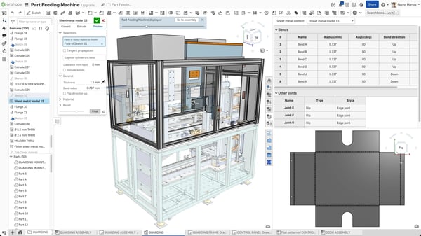
The platform’s document structure contributes to that experience. Users frequently referenced assemblies, parts, drawings, and related information being organized within a single environment. For teams already evaluating broader product data management (PDM) software, that centralized approach can simplify how engineering information is shared and maintained across projects.
Several reviewers also connected Onshape to prototyping and production workflows. Cloud-based collaboration, version visibility, and centralized design management can help reduce the kinds of communication gaps that often lead to manufacturing mistakes. For teams asking which PCB design software prevents manufacturing errors and costly design oversights effectively, Onshape’s contribution comes less from electrical analysis and more from keeping engineering teams aligned around a single source of truth.
Ease of adoption surfaced throughout the feedback as well. Multiple reviewers described learning the platform quickly despite coming from traditional CAD environments. The browser interface, structured workflows, and responsive support were often mentioned as reasons new users became productive relatively quickly.
Onshape is designed around continuous connectivity. Teams that depend on browser access, real-time collaboration, and centralized project management tend to benefit most from that model. For organizations operating in environments with inconsistent internet access, that same dependency can require additional planning before deployment.
The platform also prioritizes collaboration and version management over highly specialized engineering functionality. Some reviewers noted that certain advanced capabilities available in traditional desktop CAD environments are still evolving within the Onshape ecosystem. For teams focused on design collaboration and workflow efficiency, those considerations generally appeared secondary to the broader productivity gains.
Onshape’s strongest value comes from simplifying how engineering teams work together. By combining modeling, revision control, document management, and collaboration within a browser-based environment, it helps organizations spend less time managing files and more time moving products forward. Teams that regularly share designs across departments may find that benefit more impactful than any individual modeling feature.
What I like about Onshape:
- The G2 reviews I analyzed frequently highlighted Onshape’s browser-based collaboration, revision control, and fileless workflow as major productivity advantages over traditional CAD systems.
- A recurring strength in G2 feedback was the platform’s centralized design management and version tracking, which helps engineering teams collaborate without creating duplicate files.
What G2 users like about Onshape:
“I love the ease of design control and real-time collaboration with Onshape. It provides the best of both worlds for file control and design exploration, all while maintaining revision control and the ability to explore with branches and merge concepts back into it. It is easy to install and roll out. The training modules quickly bring new and experienced CAD users into the new tool. There is no need to maintain multiple versions of the software.”
– Onshape review, Daniel B.
What I dislike about Onshape:
- Internet connectivity comes up regularly in G2 reviews, particularly from teams working in environments where reliable online access isn’t always available.
- Engineers transitioning from traditional desktop CAD tools occasionally describe an adjustment period in G2 feedback as they adapt to Onshape’s browser-first workflow and feature set.
What G2 users dislike about Onshape:
“There isn’t really anything I dislike about Onshape, except for one issue: it relies entirely on an internet connection. If your connection is slow or unstable, the software’s performance also suffers, which can be quite frustrating.”
– Onshape review, Subhajeet S.
Best PCB design software by use case: My quick recommendations
As I analyzed G2 reviews across all seven products, the biggest differences came down to workflow priorities. Some teams needed stronger collaboration and revision control, while others focused on routing complexity, simulation depth, or manufacturing readiness. These recurring themes made it easier to identify where each product consistently delivered the most value.
|
Software |
Choose if you need to… |
Why I recommend it |
|
Altium Develop |
|
G2 users repeatedly highlighted collaboration, revision control, and engineering coordination across complex hardware projects. |
|
Altium CircuitMaker |
|
Feedback on G2 consistently positioned it as an accessible entry point for students, makers, and independent engineers. |
|
Sigrity X Platform |
|
The G2 reviews I analyzed frequently centered on SI/PI analysis, simulation accuracy, and early-stage design validation. |
|
Allegro X PCB Designer |
|
Reviewers on G2 often connected Allegro X with advanced routing control, constraint management, and manufacturing readiness. |
|
Autodesk Fusion |
|
Across the G2 feedback, users frequently praised its ability to unify CAD, CAM, simulation, and product-development workflows. |
|
PADS Professional |
|
G2 reviewers regularly referenced routing efficiency, HyperLynx integration, and validation-focused design workflows. |
|
Onshape |
|
Customer feedback on G2 consistently emphasized browser-based collaboration, version control, and design transparency. |
Frequently asked questions (FAQs) about the best PCB design software
Got more questions? G2 has the answers.
Q1. How do I design a PCB?
To design a PCB, start with a schematic that defines component connections, then convert it into a board layout using PCB design software. After placing components and routing traces, validate the design and generate manufacturing files such as Gerbers.
Q2. Can I design a PCB on mobile?
Yes, some PCB design applications support mobile devices, but most are intended for basic editing and review tasks. For advanced routing, simulation, validation, and manufacturing preparation, desktop-based PCB design platforms remain the preferred choice.
Q3. How do I learn PCB design?
Most engineers learn PCB design by combining electronics fundamentals with hands-on practice. Start with simple schematics and layouts, then gradually explore routing, signal integrity, manufacturing constraints, and design validation using beginner-friendly PCB design software.
Q4. How do I choose the right PCB layout design for my project?
The right PCB layout depends on board complexity, layer count, component density, signal requirements, and manufacturing constraints. High-speed or high-density projects often require stronger routing, simulation, and validation capabilities than simpler designs.
Q5. Which is the best free PCB design software?
Altium CircuitMaker is one of the most popular free PCB design platforms for students, makers, and hobbyists. It provides schematic capture, PCB layout, community support, and professional design concepts without requiring a commercial software investment.
Q6. Which design tools support team collaboration and design review workflows for your workflow?
Based on the G2 reviews I analyzed, Altium Develop and Onshape stood out for collaboration, revision control, and design review workflows. Both platforms help distributed engineering teams manage changes, maintain visibility, and coordinate work more effectively.
Q7. What is the most reliable PCB design software by electrical engineers based on user reviews?
Altium Develop, Autodesk Fusion, and Onshape earned some of the strongest satisfaction scores in the category. G2 reviewers frequently praised their reliability, ease of use, workflow consistency, and ability to support long-term engineering projects.
Q8. What is the highest rated PCB design for complex boards ensuring first-time manufacturing success rates?
Sigrity X Platform, Allegro X PCB Designer, and PADS Professional received the strongest feedback for handling complex boards. Their simulation, validation, routing, and constraint-management capabilities help engineering teams reduce costly design revisions before production.
Q9. What is the most trusted PCB design by practitioners in similar industries based on user reviews?
Trust often depends on industry requirements, but Altium Develop, Autodesk Fusion, and Onshape consistently earned strong ratings across engineering, manufacturing, and product-development teams. Their broad adoption and positive reviewer sentiment reinforce that trust.
Q10. What is the best PCB design software for hardware engineers designing complex circuit boards for your team?
Hardware teams working on sophisticated electronics frequently favor Altium Develop, Allegro X PCB Designer, and PADS Professional. G2 reviewers highlighted their advanced routing, component management, design validation, and workflow-control capabilities for demanding projects.
Q11. Which circuit board design platforms provide accurate simulation and manufacturing validation for your team?
Sigrity X Platform and PADS Professional received the strongest review-based recognition for simulation and validation workflows. Engineers frequently referenced signal integrity analysis, power integrity evaluation, and pre-manufacturing verification as major strengths.
Q12. What are the best PCB design tools for electronics teams reducing design iterations?
PADS Professional, Sigrity X Platform, and Allegro X PCB Designer were repeatedly associated with identifying issues earlier in the design cycle. Their validation, simulation, and constraint-management capabilities help reduce unnecessary redesign work.
Q13. Which PCB design software provides signal integrity analysis and design validation for your workflow?
Sigrity X Platform is the strongest fit when signal integrity and power integrity analysis are primary priorities. G2 reviewers consistently connected the platform to high-speed design validation, electrical performance analysis, and manufacturing readiness.
Q14. Which PCB design platforms offer seamless CAM output for manufacturing handoff for your workflow?
Autodesk Fusion, PADS Professional, and Allegro X PCB Designer were frequently associated with manufacturing preparation. Reviewers highlighted CAM integration, production workflows, Gerber generation, and design-to-manufacturing continuity as recurring strengths.
Q15. Which PCB design software prevents manufacturing errors and costly design oversights effectively?
No platform eliminates risk entirely, but G2 reviewers frequently connected Sigrity X Platform, PADS Professional, and Allegro X PCB Designer with stronger validation workflows. Their simulation, verification, and constraint-management features help identify issues before fabrication.
Better boards start with better design decisions
The biggest mistake buyers make is assuming every PCB platform solves the same problem. It doesn’t. The category includes tools built for very different priorities, from collaboration and version control to signal integrity analysis, manufacturing validation, and complex routing.
That’s why the best PCB design software is usually the one that addresses the engineering challenge creating the most friction today.
The same principle applies when evaluating the most trusted PCB design by practitioners in similar industries based on user reviews. The strongest option is rarely the platform with the most features. It’s the one that aligns most closely with your workflow, team structure, and design requirements.
Before sending designs to manufacturing, reduce risk by validating performance, signal behavior, and design integrity with simulation and test suites. Catching issues earlier is often far less expensive than discovering them after production begins.

💸 Earn Instantly With This Task
No fees, no waiting — your earnings could be 1 click away.
Start Earning
